LED Screen Manufacturing ,The Ultimate Guide to LED Screen Manufacturing: Processes, Quality Control, and Cutting-Edge Innovations
Published: 29 Apr 2025
🌐 LED Screen Manufacturing: A Deep Dive into Processes, Quality, and Innovation
LED Screen Manufacturing , LED screens are everywhere—from smartphones to stadium billboards. But what goes into making these dazzling displays? This guide unpacks every step of LED screen manufacturing, including production processes, quality control, and manufacturing innovations, with visuals to bring the journey to life.
🏭 Section 1: LED Screen Production Processes
1.1 Design and Prototyping
Engineers using CAD software to design LED modules

Every LED screen begins with meticulous design. Engineers use 3D CAD tools to model circuitry, pixel layouts, and thermal systems. Prototypes undergo stress tests for:
- Pixel Density: Balancing resolution with energy consumption (e.g., 1.2mm vs. 2.5mm pitch).
- Material Science: Selecting substrates (e.g., FR-4 PCBs) and LED types (SMD vs. COB).
- Thermal Simulations: Predicting heat dissipation to avoid hotspots.
1.2 PCB Fabrication

The PCB is the display’s nervous system. LED Screen Manufacturing steps include:
- Lamination: Layering fiberglass and copper foil.
- Photolithography: UV light transfers circuit patterns onto the board.
- Etching: Chemical baths remove excess copper, leaving precise traces.
- Drilling: Laser drills create micro-vias for component connections.
Advanced Tip:
For ultra-thin displays, manufacturers use flexible PCBs made of polyimide, which can bend without breaking. For more information about “led display materials explained” in details
1.3 LED Chip Mounting
LEDs are mounted using two primary methods:
- Surface-Mount Technology (SMT): High-speed pick-and-place robots position 10,000+ LEDs per hour with ±0.01mm accuracy.
- Chip-on-Board (COB): Bare LED chips are bonded directly to the PCB, then coated with phosphor for color uniformity.
Pro Insight:
COB technology eliminates the “grid effect” (visible gaps between pixels), making it ideal for fine-pitch displays.
1.4 Soldering and Reflow
- Reflow Soldering: Boards pass through a 7-zone oven, heating solder paste to 250°C for seamless bonding.
- Selective Soldering: For mixed SMT and through-hole components, targeted nozzles apply solder.
Quality Hack:
Nitrogen gas is injected into ovens to prevent oxidation, ensuring shiny, reliable solder joints.
1.5 Module Assembly
Modules (typically 8×8 inches) are built by:
- Encapsulation: Applying silicone or epoxy resin to shield LEDs from moisture and UV rays.
- Driver Installation: Integrating constant-current drivers to maintain brightness consistency.
Fun Fact:Outdoor screens use conformal coating-a waterproof layer that withstands rain and dust.
1.6 Final Assembly and Calibration
Modules are combined into larger panels (e.g., 46×46 inches) and calibrated for:
- Color Uniformity: Using spectrophotometers to adjust RGB values across the screen.
- Gamma Correction: Fine-tuning brightness gradients for accurate grayscale.
Case Study:
Broadcast studios use 3D LUTs (Look-Up Tables) to ensure on-screen colors match real-life hues.
1.7 Testing and Packaging
- Burn-In Tests: Screens run for 72+ hours at maximum brightness to weed out infant mortality failures.
- IP Testing: Spraying water jets (IP65) or dust chambers (IP6X) to validate durability.
- Packaging: Foam-lined crates with humidity indicators for international shipping.
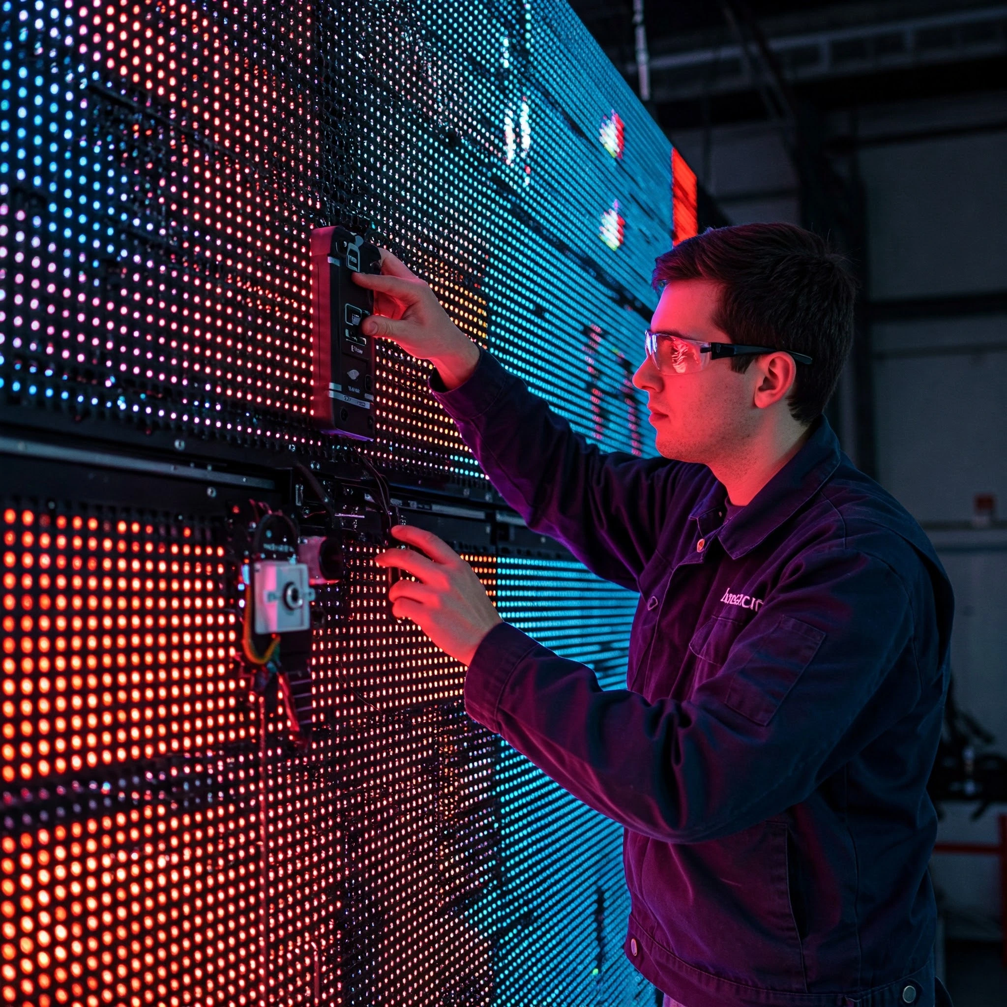
🔍 Section 2: Quality Control in LED Screen Manufacturing
2.1 In-Line Inspections
AOI Systems: Cameras check for missing components, tombstoning (lifted LEDs), and solder defects at 50μm resolution.
- X-Ray Inspection: Detecting hidden flaws like voiding in solder balls.
Industry Standard in LED Screen Manufacturing:
Top manufacturers maintain a Defects Per Million (DPM) rate below 50.
2.2 Electrical and Optical Testing
- Electrical Tests:
- Forward Voltage Checks: Ensuring LEDs operate within 2.8–3.4V range.
- Leakage Current Tests: Preventing power drain in standby mode.
- Optical Tests:
- Luminance Uniformity: ≤5% variance across the screen.
- Color Gamut: Achieving 100% NTSC or DCI-P3 standards.
2.3 Environmental Stress Testing
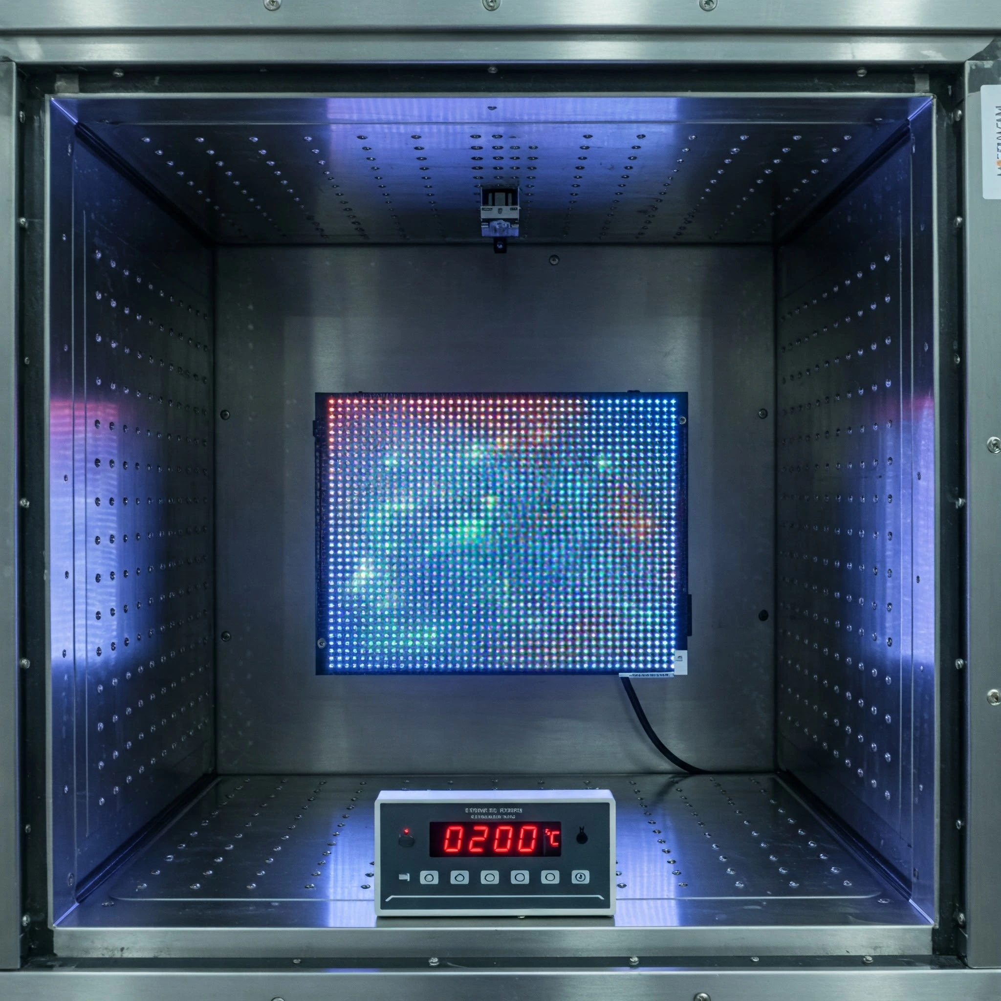
Screens undergo brutal simulations:
- Thermal Shock: Cycling between -40°C and 85°C to test material expansion.
- Salt Spray Tests: For coastal installations, verifying corrosion resistance.
Real-World Example: Airport displays endure 90% humidity tests to handle condensation from frequent door openings.
2.4 Certifications and Compliance
- RoHS: Bans lead, mercury, and cadmium.
- ENERGY STAR: Validates energy efficiency for consumer displays.
🚀 Section 3: Innovations in LED Screen Manufacturing
3.1 Micro-LED Breakthroughs
Image Suggestion: Micro-LEDs under a microscope (Alt Text: Micro-LED technology close-up)
- Mass Transfer: Using stamp-like tools to place millions of < 100μm LEDs onto substrates.
- Self-Emissive Design: No backlight = infinite contrast ratios (perfect for HDR).
Use Case:
Samsung’s The Wall uses modular Micro-LEDs for customizable screen sizes.
3.2 Flexible and Transparent Displays
- Rollable Screens: LG’s 65-inch OLED-like LED TV rolls into a box.
- Transparent LED Films: 70% transparency for retail windows (e.g., Sony’s Crystal LED).
Material Science:Graphene-based electrodes enable ultra-thin, bendable displays.
3.3 AI Automation
AI robot inspecting LED modules

- Predictive Maintenance: AI monitors machinery to prevent downtime.
- Generative Design: Algorithms create optimal heat dissipation patterns.
Stat Alert:
Smart factories
3.5 Quantum Dot and Nano Innovations
- QD Enhancement Films: Boosting color gamut to 140% sRGB.
- NanoBarrier Coatings: Blocking oxygen/water ingress to extend lifespan.
❓ FAQ: LED Screen Manufacturing
Precision manufacturing, rare materials (e.g., gallium nitride), and rigorous testing drive costs.
Yes! Individual modules can be replaced without dismantling the entire screen.
Blue LEDs coated with yellow phosphor create white light; red/green phosphors adjust color temps
Yes! Brands like Samsung use solar-powered factories and recyclable packaging.
100,000+ hours (11+ years) for indoor screens; 50,000 hours for outdoor due to environmental stress.
🎯 Conclusion
LED screen manufacturing is a symphony of engineering precision, relentless quality checks, and bold innovation. As technologies like Micro-LED and AI automation redefine possibilities, the future promises thinner, brighter, and greener displays. Whether you’re a tech geek or a business buyer, understanding these intricacies helps you make informed choices-and marvel at the science behind every pixel.
🔧 Lighting the Way Forward: Stay curious, stay updated!


- Be Respectful
- Stay Relevant
- Stay Positive
- True Feedback
- Encourage Discussion
- Avoid Spamming
- No Fake News
- Don't Copy-Paste
- No Personal Attacks
- Be Respectful
- Stay Relevant
- Stay Positive
- True Feedback
- Encourage Discussion
- Avoid Spamming
- No Fake News
- Don't Copy-Paste
- No Personal Attacks
